About Hologenix
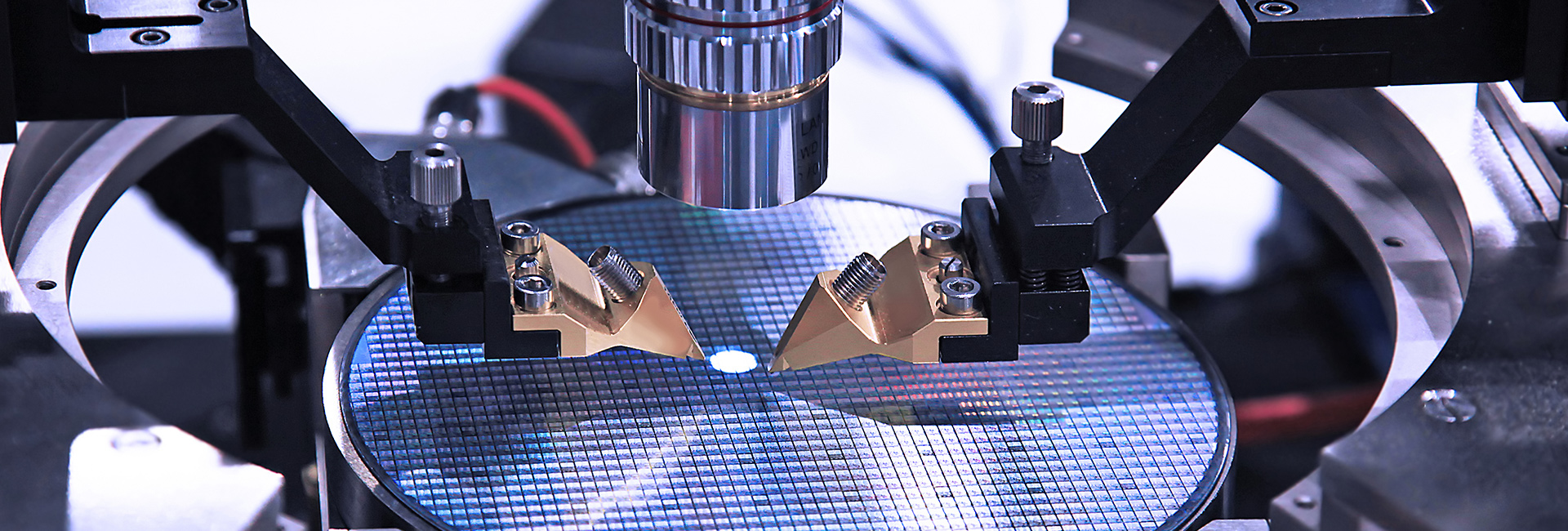
Shortly after Hologenix first introduced the Magic Mirror surface inspection method to the semiconductor industry it became a standard in silicon wafer manufacturing. By 1995 the major silicon suppliers and many integrated device manufacturers were using this novel technology in QC/QA. Hologenix has continued to develop, introduce and apply innovative products for inspection, metrology, test, and production in diverse industries. Innovative software and systems such as the MX Gauges by E+H, Boin's award-winning WAFERMAP software, the YSS Solar Simulators by Yamashita Denso, and Hologenix's own NGS advanced metrology system, are used in critical high-tech applications worldwide.
Since our start-up days in the early 90's, Hologenix has built an extensive network of domestic and international business partners, including OEMs, systems integrators, vendors, distributors and research institutes. We participate in international conferences and symposiums for advanced technologies in diverse industries. Hologenix is located 40 minutes south of the Los Angeles International Airport in an R&D park adjacent to Boeing Space Systems. With a variety of equipment on site, we are able to perform application support and measurement services.
Hologenix Featured Products


Hologenix, Huntington Beach California